Can Fine-Pitch Hybrid Bonding Go High Volume?
Original reporting by Semiconductor Engineering
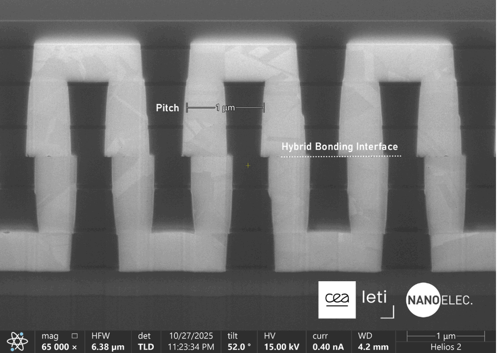
Hybrid bonding refers to a critical advanced packaging technology that directly joins prepared copper and dielectric surfaces to create high-density electrical interconnects between chips. While already proven in some wafer-to-wafer applications like image sensors, its most transformative applications involve fine-pitch, die-to-wafer integration, combining diverse components like logic and memory. This transition, however, presents an extraordinary manufacturing challenge, demanding precision beyond current industry norms.
The Integration Hurdle Achieving high-volume production for fine-pitch die-to-wafer hybrid bonding requires maintaining a consistent, minuscule process window across an entire ecosystem of fabs, OSATs, equipment, and materials. Every step, from upstream fabrication and surface preparation to individual die handling, alignment, and bonding, contributes to a cumulative error budget. Particle contamination, material stress, wafer warpage, and precise die placement become magnified issues as interconnect pitches shrink to a few microns. Furthermore, the high temperatures typically needed for annealing these bonds can be incompatible with sensitive components, driving the need for lower-thermal budget solutions. Success hinges on a deeply integrated approach that addresses these interconnected challenges, transforming a working lab process into a scalable, repeatable, and economically viable manufacturing reality.
Hybrid bonding stands as a foundational technology for advanced packaging, yet its full potential in fine-pitch, die-to-wafer integration hinges on surmounting a complex web of interconnected manufacturing challenges. The transition from established wafer-to-wafer processes to the exquisite precision required for heterogeneous chiplet integration demands not just incremental improvements, but a holistic re-evaluation of every step—from microscopic particle control and surface topography to precise alignment, placement accuracy, and carefully managed thermal budgets. Achieving high-volume manufacturing (HVM) is less about perfecting individual process steps and more about ensuring their collective stability, maintaining an exquisitely narrow process window across diverse suppliers, equipment, and company boundaries. Each microscopic deviation, whether from film stress, material mismatch, or placement error, accumulates, threatening the yield of increasingly valuable and complex assemblies. This collective variation, more than any single parameter, represents the ultimate barrier to widespread adoption.
Redefining Integration
Overcoming these hurdles will fundamentally redefine the landscape of semiconductor manufacturing. Successful scaling of fine-pitch hybrid bonding promises to unlock unprecedented levels of heterogeneous integration, enabling advanced functionality and performance gains previously unattainable. This paradigm shift will accelerate the development of next-generation AI accelerators, high-bandwidth memory stacks, and complex system-in-package solutions, driving innovation across industries from autonomous vehicles to edge computing. The meticulous control required for this technology also fosters a new era of collaborative manufacturing, where integrated data analytics and shared process understanding become critical for success, pushing the boundaries of what integrated circuits can achieve. Ultimately, the future of advanced packaging, and indeed the trajectory of semiconductor performance, will be shaped by the industry's ability to transform the intricate art of hybrid bonding into a consistently repeatable, high-volume science.
Frequently asked questions
- What is hybrid bonding, and why is it important for future semiconductor devices?
- Hybrid bonding is a direct chip-to-chip or chip-to-wafer interconnection technology that directly joins copper and dielectric surfaces. It enables extremely dense interconnections, crucial for stacking heterogeneous components like logic and memory in advanced packages. However, achieving high-volume manufacturing is challenging due to extreme sensitivity to particles, surface imperfections, precise alignment requirements, and the need for a consistent process window across many manufacturing steps.
- How does die-to-wafer hybrid bonding differ from wafer-to-wafer bonding in chip production?
- Wafer-to-wafer bonding joins entire patterned wafers in parallel, offering high throughput but requiring both wafers to have high yield. Die-to-wafer bonding, by contrast, individually picks, aligns, and places known-good dies onto a target wafer. This allows for pre-screening to improve final product yield but introduces complexities and slower throughput due to repeated handling and precise alignment of each individual die.
- What manufacturing hurdles must be overcome to enable widespread adoption of fine-pitch hybrid bonding?
- Widespread adoption requires overcoming several critical manufacturing hurdles. Extreme cleanliness is paramount, as even nano-sized particles can prevent proper bonding. Precise alignment and control over subtle surface variations, film stress, and wafer warpage are also crucial, especially at fine pitches where tolerances are minimal. Furthermore, ensuring a compatible, low-temperature bonding process is essential for integrating heat-sensitive components without damage.