AI Models Transform Defect Inspection And Review, But Can Fail To Scale
Original reporting by Semiconductor Engineering
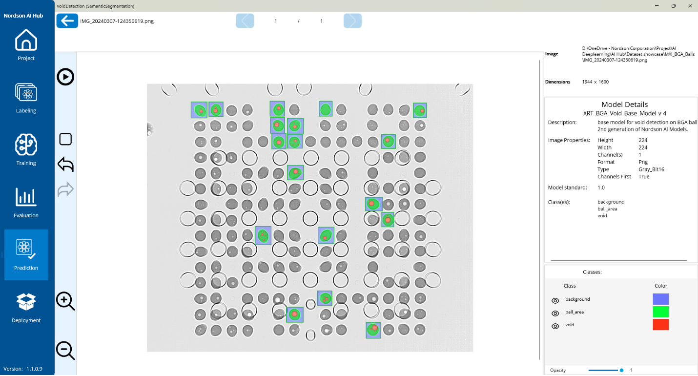
Artificial intelligence is rapidly transforming semiconductor manufacturing, offering a powerful new lens to combat the myriad defects plaguing complex process steps. From lithography to advanced packaging, AI models are proving instrumental in distinguishing critical yield-killing flaws from nuisance defects, and even unearthing imperfections previously invisible to traditional methods. This pattern recognition capability is particularly vital as new techniques like hybrid bonding introduce unique defect signatures, especially at the critical wafer edge, where AI-powered inspection is now proving essential for maintaining high yields.
The scaling hurdle Despite these undeniable successes, deploying AI solutions beyond initial pilot projects remains a formidable challenge for the industry. A staggering 70% of AI initiatives falter after successful trials, primarily due to fragmented data, legacy factory systems, and the immense task of establishing robust data infrastructure. While AI excels at defect classification and is even beginning to enhance metrology, its true potential is hampered by the often-overlooked, painstaking work of collecting, aligning, and normalizing data across the entire manufacturing lifecycle. Overcoming these integration hurdles, rather than just developing sophisticated algorithms, will be key to unlocking AI's full enterprise-wide impact, swiftly identifying and rectifying root causes for sustained yield improvement.
AI's undeniable value in semiconductor manufacturing lies in its capacity to revolutionize defect detection and yield improvement. From distinguishing subtle nuisance defects to revealing previously invisible anomalies at the wafer edge, AI-driven inspection and classification models are enhancing precision and accelerating process learning. While traditionally excelling in pattern recognition for inspection, AI's role in metrology is evolving, particularly in signal reconstruction, process modeling, and accelerating complex computations, boosting performance at advanced nodes. The industry is witnessing a trend toward more intuitive models that streamline programming needs, improving outlier identification and root cause analysis when integrated with robust data infrastructure. However, the true bottleneck remains not the models themselves, but the foundational work of seamlessly integrating disparate data sources across the entire manufacturing lifecycle.
The Road Ahead
This persistent challenge of data connectivity underscores the broader implications of AI's integration. As companies overcome fragmented data, leverage advanced platforms, and align metadata standards, the future of semiconductor manufacturing will be characterized by unprecedented levels of automation, precision, and efficiency. AI promises to transform everything from early design stages through to field deployment, enabling faster iteration, proactive issue resolution, and the successful scaling of advanced packaging and new process nodes crucial for next-generation devices. Ultimately, the widespread deployment of AI will hinge on moving beyond isolated pilot projects to establish a fully integrated, intelligent manufacturing ecosystem. Here, real-time, correlated insights will drive rapid, informed decision-making, fulfilling AI's potential to usher in an era of continuous innovation and resilience for a complex, data-intensive industry.
Frequently asked questions
- How is artificial intelligence improving semiconductor manufacturing processes and defect detection?
- Artificial intelligence significantly enhances semiconductor manufacturing by revolutionizing defect detection and yield improvement. It excels at identifying critical flaws, distinguishing them from minor imperfections, and even revealing defects previously invisible to traditional methods. This capability is crucial for complex processes like lithography and advanced packaging, especially at the wafer edge, ensuring higher quality and efficiency in chip production.
- What are the main challenges in deploying AI in semiconductor factories?
- Deploying AI solutions beyond initial pilot projects in semiconductor manufacturing faces significant hurdles. A primary challenge is fragmented data, coupled with legacy factory systems and the immense task of establishing robust data infrastructure. The painstaking work of collecting, aligning, and normalizing data across the entire manufacturing lifecycle often bottlenecks AI's full potential, leading to many initiatives faltering after successful trials.
- How will AI transform the future of semiconductor manufacturing and its overall ecosystem?
- AI promises to transform semiconductor manufacturing by ushering in unprecedented levels of automation, precision, and efficiency. By overcoming data fragmentation and integrating disparate sources, AI will enable faster design iterations, proactive issue resolution, and successful scaling of advanced packaging and new process nodes. This will lead to a fully integrated, intelligent manufacturing ecosystem where real-time insights drive rapid decision-making and continuous innovation.